DIY-Calculator Hardware:Community Portal
From DIY-Calculator_Hardware
(Difference between revisions)
| Revision as of 23:30, 18 July 2006 Diy-admin (Talk | contribs) ← Previous diff |
Revision as of 09:02, 19 July 2006 Jh (Talk | contribs) Next diff → |
||
| Line 12: | Line 12: | ||
| == Hardware Project == | == Hardware Project == | ||
| - | Block diagram of the PCB: | + | Block diagram of the PCB: [[Image:Blockdiagram.jpg|thumb|left]] |
| - | [[Image:Blockdiagram.jpg]] | + | |
| + | |||
| + | |||
| + | |||
| + | |||
| + | |||
| + | |||
| + | |||
| + | |||
| + | |||
| + | |||
| + | |||
| + | |||
| + | |||
| + | |||
| + | |||
| + | Download the schematics from here: [[Image:schematics.pdf]] | ||
| + | |||
| + | |||
| == FPGA Project == | == FPGA Project == | ||
Revision as of 09:02, 19 July 2006
The DIY Calculator Hardware Project consists of several sub projects:
- Creating the real hardware: a printed circuit board (PCB) with the processing chips, an LCD module, switches, and connectivity to a host computer
- Implementing the DIY Calculator CPU together with supporting functional blocks within a programmable logic chip (a so-called "Field Programmable Gate Array" - FPGA).
- Writing the firmware running on the hardware, including a ROM monitor
- Adding a software tool for communicating with the hardware (e.g. uploading user programs)
On this page you will find information about the progress of the project as well as technical details.
Contents |
Hardware Project
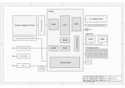
Block diagram of the PCB:
Download the schematics from here: Image:Schematics.pdf


