DIY-Calculator Hardware:ROM Monitor Project
From DIY-Calculator_Hardware
Revision as of 14:29, 14 October 2006
On of the primary goals of the DIY Calculator project is to teach how computers are working on machine language level ("How Computers Do Math"). So everyone is highly encouraged to translate various algorithms into assembly programs for the DIY Calculator. The current virtual DIY Calculator comes with a ready-to-use environment, which includes the calculator-like user interface, an assembler, a simulator, single-step debugger, and memory and register display. When translating the design to a physical one there has to be an environment, too. The most important functionality (and this is the only one being in scope of this project) is to run user programs to the DIY Calculator hardware. To be able to do that there must be means of:
- uploading the program to the hardware
- store it in some non-volatile storage
- actually run it
- obtain some status information (e.g. terminated correctly, does not fit into memory, etc.)
This is the objective of the ROM monitor. The ROM monitor is, as its name suggests, a program which resides within the ROM of the DIY Calculator. It is always present there and provides for the above mentioned supervising tasks. It uses the RS-232 port both for transferring the user program and as console port to which you can connect with a terminal emulation program (or a real "dumb" terminal if can get hold of one ..) to enter commands and display status information. The ROM monitor will be written in the DIY Calculator's assembly language and will additionally supply some basic functions (e.g. status/log output via RS-232) to user programs.
Project status (19.Jul.2006): basic conceptual design ready
Project status (7.Aug.2006): no changes
Project status (31.Aug.2006): no changes
Project status (6.Sep.2006): work started
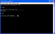
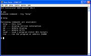
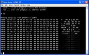
Project status (12.Sep.2006): First time that a program has been loaded and run to the DIY Calculator successfully! See terminal screen shot:
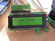
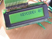
I loaded this program: keycode.lst, which waits for a key press and then displays the key code. Download the .ram file (keycode.ram) and load it into your virtual DIY Calculator. In the real world you press buttons on the PCB and the codes are displayed on the LCD:
Project status (13.Sep.2006): support of the DIY Calculator native hex format (.ram files).
Project status (15.Sep.2006): working on interrupt code - stay tuned!
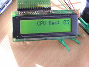
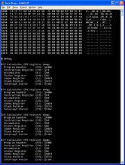
Project status (19.Sep.2006): UART Rx interrupt now works reliable. First steps with Single-Step interrupt are promising - see screen shot:
Project status (22.Sep.2006): Single-Step and Run buttons work! Clive (Maxfield) contributed the assembler code for it and after finding a basic obscurity inside the interrupt structure it worked out of the box with only a few minor flaws. Thank you, Max!
Thanks to that it is now possible to load a program and single-step debug it on the real hardware!
See the program listing and the terminal log (with remarks): simpled.lst simpled-debug.txt
To end a debug session press either 'Run' to run the program or you press 'Reset' for a hard reset or you press 'CTRL-C' on the terminal for a soft reset.
Project status (9.Oct.2006): Added access to the configuration flash ROM of the FPGA (see FPGA part). There are three new commands for managing the flash:
- 'cpflash [address] [# of bytes]': copies # bytes from RAM to flash, starting ad address
- 'cpram [address] [# of bytes]': copies # bytes from flash to RAM, starting at address
- 'eflash': erases the flash
More information on flash usage: The FPGA is based on a volatile storage technology (SRAM cells). Thus it has to be loaded (or configured) each time power is applied. This can be done using several different mechanisms, one of the easiest is using a serial (flash) PROM which contents is automatically loaded into the FPGA by some hard-wired logic inside the FPGA after power-on. The amount of memory needed inside the flash ROM is determined by the size of the FPGA. The FPGA chip we use on the DIY Calculator is a Lattice LFEC10E chip requiring about 3.1Mbit storage. It depends on the used flash memory how much free space remains. The free space can be used to store user data. The memory inside the flash is sectorized with 64KB each sector. We use the topmost sector for storing the user program that is intended to run on the DIY Calculator. During a hard reset all RAM is restored from flash. When erasing the flash only the topmost sector is erased, keeping FPGA configuration information. Likewise, when writing to the flash the sector address is fixing thus preventing overwriting vital FPGA config data.
