DIY-Calculator Hardware:FPGA Project
From DIY-Calculator_Hardware
| Revision as of 16:44, 11 December 2006 Jh (Talk | contribs) ← Previous diff |
Revision as of 17:00, 11 December 2006 Jh (Talk | contribs) Next diff → |
||
| Line 19: | Line 19: | ||
| [[Image:keypad_idle2.jpg|thumb|left|keypad idle]] | [[Image:keypad_idle2.jpg|thumb|left|keypad idle]] | ||
| <br style="clear:left;" /> | <br style="clear:left;" /> | ||
| - | The first signal is the keyclock output from the FPGA. The X and Y signals are the delayed key clock fed back to the FPGA. Note the timing differences among the X and Y signals. This is due to the tolerances of the threshold levels of the 74HC14 schmitt triggers. The | + | The topmost signal is the key clock output from the FPGA. The X and Y signals are the delayed key clock fed back to the FPGA. Note the timing differences among the X and Y signals. This is due to the tolerances of the threshold levels of the 74HC14 schmitt triggers. There is a margin of about 1.2usec to the sample pulse. This is sufficient for now, but maybe I have to fine tune this with the final hardware. |
| - | When you "press" a key the 220K resistor forms a delay element together with the capcitance of your finger, which will be in the 10pF range. The 10nF capacitor is much larger and can be therefore neglected. The 100K resistor is for ESD safety of the 74HC14 input. | + | When you "press" a key the 220K resistor forms a delay element together with the capacitance of your finger, which will be in the 10pF range. The 10nF capacitor is much larger and can be therefore neglected. The 100K resistor is for ESD safety of the 74HC14 input. |
| [[Image:keypad_schem.gif|thumb|left|keypad schematics]] | [[Image:keypad_schem.gif|thumb|left|keypad schematics]] | ||
| <br style="clear:left;" /> | <br style="clear:left;" /> | ||
| Line 29: | Line 29: | ||
| [[Image:keypad_active.jpg|thumb|left|active key]] | [[Image:keypad_active.jpg|thumb|left|active key]] | ||
| <br style="clear:left;" /> | <br style="clear:left;" /> | ||
| - | The delay in the X9 and the Y2 lines is clearly visible. It is detected at the rising edge of the signal "sample" and then decoded and "debounced". When a key is safely recognized, the according key code ($18 in our example) is presented at $F011 and read by the CPU. The action of reading the key code resets the keypad controller logic. You have to release the key before a new keypress can be detected. | + | The delay in the X9 and the Y2 lines is clearly visible. It is detected at the rising edge of the signal "sample" and then decoded and "debounced". When a key is safely recognized, the according key code ($18 in our example) is presented at address $F011 and read by the CPU. The action of reading the key code resets the keypad controller logic. You have to release the key before a new keypress can be detected. |
| - | View the VHDL code for the keypad controller here: [[DIY-Calculator_Hardware:Downloads|Downloads]] | + | Download the VHDL code for the keypad controller from here: [[DIY-Calculator_Hardware:Downloads|Downloads]] |
Revision as of 17:00, 11 December 2006
The PCB will contain an FPGA chip in the 10K-gates size-class (Lattice LFEC10E-3F256C) with a 256 pin BGA footprint. The included JTAG connector makes this a development board for general use. With ispLEVER, the FPGA development software suite from Lattice Semiconductor, the FPGA design can be altered or a completely new design can be made. The entry level version of ispLEVER (ispLEVER-Starter) can be downloaded freely from Lattice. With Lattice's ispVM System the design can be transferred via JTAG to the DIY Calculator PCB.
The FPGA design of the DIY Calculator is based on the work of Steven Cooper, Carl Hoggins, Bjornar Prestegard, Svein Roar Kvaale, and Dr Albert Koelmans (instructor) of the University of Newcastle Upon Tyne, England.
Additionally to the CPU and ROM and RAM there will be special logic for the switch matrix, for LCD output, and a UART for RS-232 communication to the host PC.
Project status (11.Dec.2006):
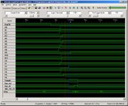
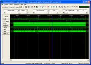
Implemented the keypad controller for the sensor keypad. View the Logic analyzer screen shots:
The topmost signal is the key clock output from the FPGA. The X and Y signals are the delayed key clock fed back to the FPGA. Note the timing differences among the X and Y signals. This is due to the tolerances of the threshold levels of the 74HC14 schmitt triggers. There is a margin of about 1.2usec to the sample pulse. This is sufficient for now, but maybe I have to fine tune this with the final hardware.
When you "press" a key the 220K resistor forms a delay element together with the capacitance of your finger, which will be in the 10pF range. The 10nF capacitor is much larger and can be therefore neglected. The 100K resistor is for ESD safety of the 74HC14 input.
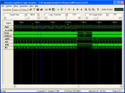
See a Logic analyzer picture when a key is activated:
The delay in the X9 and the Y2 lines is clearly visible. It is detected at the rising edge of the signal "sample" and then decoded and "debounced". When a key is safely recognized, the according key code ($18 in our example) is presented at address $F011 and read by the CPU. The action of reading the key code resets the keypad controller logic. You have to release the key before a new keypress can be detected.
Download the VHDL code for the keypad controller from here: Downloads
Project status (9.Oct.2006):
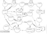
Added a controller module "SPI flashcontroller" for SPI flash ROM (FPGA configuration ROM) access (see controller state diagram)
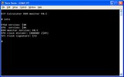
Here is the logic analyzer recording of the "Read Signature" command (with corresponding terminal log).
At cursor 'A' the command ($AB) is issued to the flash controller, afterwards the command plus 3 dummy bytes (as per flash data sheet) are transmitted to the flash via the SPI interface. During this time the CPU waits for the response. At cursor 'B' the CPU detects that a new data byte from the flash is ready (reading $06 from the status port). At cursor 'C' the response is read ($13 for the used M25P80 chip).
Project status (11.Sep.2006):
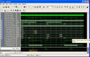
Keypad controller implemented. During work on the ROM monitor it was necessary to complete the DIY Calculator with the keypad. While the real PCB being still not available the Lattice development board features 12 buttons organized in a 3 by 4 column / row fashion. The keypad controller is currently designed with this configuration but behaves at the DIY Calculator side exactly like the virtual version does and the real version will. See modelsim screenshot:
Two key presses are simulated: first key '5' and then key '9'. See the scan rows changing (e.g. row1, row1_last) detecting changes and generating the 'key_set' signal which latches the respective key code. This in turn causes the KEYPAD input port to change from $FF to the key code ('d_out' signal). When the CPU reads from KEYPAD (short pulse on 'sel' line) a pulse on 'beep' signal is generated and the KEYPAD port value is reset to $FF.
Note (with the first key press) the '5'-key is still depressed when the CPU reads the KEYPAD but no additional key events are generated. In the second case ('9'-key) the key is released before the CPU reads KEYPAD.
Project status (6.Sep.2006):
Note the "tx_empty" signal which denotes an empty transmitter register. During the shifting-out of the character tx_empty goes low thereby indicating that the CPU must not write a next character. The CPU is busy during this phase with polling the UART status register waiting for tx_empty going high again. tx_empty may trigger an interrupt request, if enabled by software.
Line speed is 38.4 kbaud.
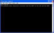
Here the "rx_ready" is signal used for CPU handshake. When a character ('U' / $55 in the picture) is received rx_ready becomes high thus indicating to the CPU that a character is available n the UART for reading. When the CPU reads the character rx_ready goes low again. In the screen shot the CPU writes then the character to the LCD, which is easy recognizable as the CPU is halted during LCD access by means of the "nWAIT" signal. View the program listing here: uart-test.lst
Line speed is (as with transmit) 38.4 kbaud.
Project status (4.Sep.2006):
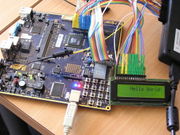
Notice that there are two access cycles to the LCD module with each character, one which actually writes the character and a second one which shifts the display left, resembling the display behaviour of desktop calculators. Also note that during LCD accesses the CPU is effectively halted by the nWAIT signal which is generated by the LCD controller. Between LCD accesses there is activity on the CPU data and address bus, which indicates the loading of the next character, etc.
View the "Hello World" program here: hello-tasm.lst
Project status (31.Aug.2006):
new CPU design is ready! (simulated and tested in a Lattice FPGA development board.)
Download the VHDL code from here: Downloads
Next steps are design/integration of:
- LCD controller
- UART
- Keypad controller
- stay tuned!
Project status (7.Aug.2006):
Simulation of the existing CPU design revealed big troubles. A new design of the CPU is being made.
Project status (19.Jul.2006):
concept proved, integration of the existing VHDL design (was done with Altera/Quartus) into ispLEVER


