DIY-Calculator Hardware:Community Portal
From DIY-Calculator_Hardware
The DIY Calculator Hardware Project consists of several sub projects:
- Creating the real hardware: a printed circuit board (PCB) with the processing chips, an LCD module, switches, and connectivity to a host computer
- Implementing the DIY Calculator CPU together with supporting functional blocks within a programmable logic chip (a so-called "Field Programmable Gate Array" - FPGA).
- Writing the firmware running on the hardware, including a ROM monitor
- Adding a software tool for communicating with the hardware (e.g. uploading user programs)
On this page you will find information about the progress of the project as well as technical details.
Contents |
Hardware Project
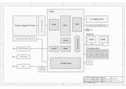
Block diagram of the PCB:
The layout will somewhat resemble the layout of the (virtual) DIY Calculator with an 20x1 character LC display and a 70 keys sensor key matrix. Additionally there are connectivity means for a host PC:
- serial RS-232 for uploading user programs and providing a console to the DIY Calculator CPU
- a JTAG programming connector; this connects to the PC's parallel port and enables the user to load new designs into the FPGA
Additionally there will be sockets for external ROM/RAM chips and a large prototyping area for free use.
Download the detailed schematics from here: Image:Schematics.pdf
Project status (19.Jul.2006): schematics completed, PCB layout work started
FPGA Project
The PCB will contain an FPGA chip in the 10K-gates size-class (Lattice LFEC10E-3F256C) with a 256 pin BGA footprint. The included JTAG connector makes this a development board for general use. With ispLEVER, the FPGA development software suite from Lattice Semiconductor, the FPGA design can be altered or a completely new design can be made. The entry level version of ispLEVER (ispLEVER-Starter) can be downloaded freely from Lattice. With Lattice's ispVM System the design can be transferred via JTAG to the DIY Calculator PCB.
The FPGA design of the DIY Calculator is based on the work of Steven Cooper, Carl Hoggins, Bjornar Prestegard, Svein Roar Kvaale, and Dr Albert Koelmans (instructor) of the University of Newcastle Upon Tyne, England.
Additionally to the CPU and ROM and RAM there will be special logic for the switch matrix, for LCD output, an a UART for RS-232 communication to the PC host.


