DIY-Calculator Hardware:Community Portal
From DIY-Calculator_Hardware
The DIY Calculator Hardware Project consists of several sub projects:
- Creating the real hardware: a printed circuit board (PCB) with the processing chips, an LCD module, switches, and connectivity to a host computer
- Implementing the DIY Calculator CPU together with supporting functional blocks within a programmable logic chip (a so-called "Field Programmable Gate Array" - FPGA).
- Writing the firmware running on the hardware, including a ROM monitor
- Adding a software tool for communicating with the hardware (e.g. uploading user programs)
On this page you will find information about the progress of the project as well as technical details.
Contents |
Hardware Project
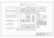
Block diagram of the PCB:
The layout will somewhat resemble the layout of the (virtual) DIY Calculator with an 20x1 character LC display and a 70 keys sensor key matrix. Additionally there are connectivity means for a host PC:
- serial RS-232 for uploading user programs and providing a console to the DIY Calculator CPU
- a JTAG programming connector; this connects to the PC's parallel port and enables the user to load new designs into the FPGA
Additionally there will be sockets for external ROM/RAM chips and a large prototyping area for free use.
Download the detailed schematics from here: Image:Schematics.pdf
Project status (19.Jul.2006): schematics completed, PCB layout work started
FPGA Project
The PCB will contain an FPGA chip in the 10K-gates size-class (Lattice LFEC10E-3F256C) with a 256 pin BGA footprint. The included JTAG connector makes this a development board for general use. With ispLEVER, the FPGA development software suite from Lattice Semiconductor, the FPGA design can be altered or a completely new design can be made. The entry level version of ispLEVER (ispLEVER-Starter) can be downloaded freely from Lattice. With Lattice's ispVM System the design can be transferred via JTAG to the DIY Calculator PCB.


