DIY-Calculator Hardware:Hardware Project
From DIY-Calculator_Hardware
(Difference between revisions)
| Revision as of 08:17, 22 October 2006 Hzulu (Talk | contribs) ← Previous diff |
Revision as of 08:18, 22 October 2006 Hzulu (Talk | contribs) Next diff → |
||
| Line 3: | Line 3: | ||
| * Serial (RS-232) for uploading user programs and providing a console to the DIY Calculator CPU | * Serial (RS-232) for uploading user programs and providing a console to the DIY Calculator CPU | ||
| * A JTAG programming connector; this connects to the PC's parallel port and enables the user to load new designs into the FPGA | * A JTAG programming connector; this connects to the PC's parallel port and enables the user to load new designs into the FPGA | ||
| - | <br style="clear:left;"> | ||
| <br style="clear:left;"> | <br style="clear:left;"> | ||
Revision as of 08:18, 22 October 2006
The layout will somewhat resemble the layout of the (virtual) DIY Calculator with an 20x1 character LC display and a 70 keys sensor key matrix. Additionally there are connectivity means for a host PC:
- Serial (RS-232) for uploading user programs and providing a console to the DIY Calculator CPU
- A JTAG programming connector; this connects to the PC's parallel port and enables the user to load new designs into the FPGA
Project status (9.Oct.2006):
New LCD module tested and integrated. The originally planned 20x1 LCD module is hard to get, so we evaluated additionally 20x2 types (this mainly has impact on the mechanical hardware design).
Project status (31.Aug.2006):
Project status (13.Aug.2006):
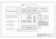
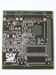
Prototype PCB layout completed. Here are the "final" schematics:
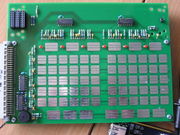
keypad mechanics:
and the layout:
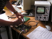
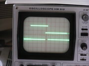
Test of sensor keypad is in progress.
Project status (7.Aug.2006):
Project status (19.Jul.2006):
schematics completed, PCB layout work started
- preliminary Schematics
