DIY-Calculator Hardware:Hardware Project
From DIY-Calculator_Hardware
| Revision as of 11:09, 15 November 2006 Hzulu (Talk | contribs) ← Previous diff |
Revision as of 11:13, 15 November 2006 Hzulu (Talk | contribs) Next diff → |
||
| Line 23: | Line 23: | ||
| After successful tests with prototype, we now changed throughhole components to SMT. Silkprint was added and 16 spare signals from FPGA board are now tied to testpoints, for better usability as a generic FPGA prototyping environment. Circuitry for switching LCD backlight was added (see new schematics). | After successful tests with prototype, we now changed throughhole components to SMT. Silkprint was added and 16 spare signals from FPGA board are now tied to testpoints, for better usability as a generic FPGA prototyping environment. Circuitry for switching LCD backlight was added (see new schematics). | ||
| - | Due to very poor availibility of the previously planned LCD Display, we decided to choose a "more common" 2x20 type. This display is manufactured by a lot of different vendors. Later the LCD controller inside the FPGA will be extended to adress the extra line - most probably a new I/O port for the CPU will be assigned for this purpose, to maintain compatibility to the Virtual DIY Calculator. | + | Due to very poor availibility of the previously planned LCD Display, we decided to choose a "more common" 2x20 type. This display is manufactured by a lot of different vendors. Later the LCD controller, inside the FPGA, will be extended to adress the extra line - most probably a new I/O port for the CPU will be assigned for this purpose, to maintain compatibility to the Virtual DIY Calculator. |
| Redesign of FPGA board is in progress... | Redesign of FPGA board is in progress... | ||
Revision as of 11:13, 15 November 2006
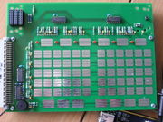
The layout will somewhat resemble the layout of the (virtual) DIY Calculator with an 20x1 character LC display and a 70 keys sensor key matrix. Additionally there are connectivity means for a host PC:
- Serial (RS-232) for uploading user programs and providing a console to the DIY Calculator CPU
- A JTAG programming connector; this connects to the PC's parallel port and enables the user to load new designs into the FPGA
Project status (15.Nov.2006):
Work on keypad revision is finished.
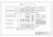
Schematics:
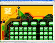
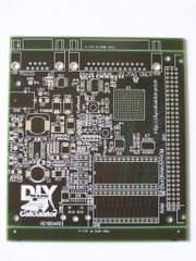
Layout:
After successful tests with prototype, we now changed throughhole components to SMT. Silkprint was added and 16 spare signals from FPGA board are now tied to testpoints, for better usability as a generic FPGA prototyping environment. Circuitry for switching LCD backlight was added (see new schematics).
Due to very poor availibility of the previously planned LCD Display, we decided to choose a "more common" 2x20 type. This display is manufactured by a lot of different vendors. Later the LCD controller, inside the FPGA, will be extended to adress the extra line - most probably a new I/O port for the CPU will be assigned for this purpose, to maintain compatibility to the Virtual DIY Calculator.
Redesign of FPGA board is in progress...
Project status (11.Nov.2006):
During the past weeks a lot of things happened at the software side (see Upload_Utility_Project). This happened just in time, since we expect the first pieces of the real DIY Calculator hardware for next week. So stay tuned, this section will soon have great news and exciting pictures!
Project status (9.Oct.2006):
New LCD module tested and integrated. The originally planned 20x1 LCD module is hard to get, so we evaluated additionally 20x2 types (this mainly has impact on the mechanical hardware design).
Project status (31.Aug.2006):
Project status (13.Aug.2006):
Prototype PCB layout completed. Here are the "final" schematics:
keypad mechanics:
and the layout:
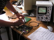
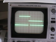
Test of sensor keypad is in progress.
Project status (7.Aug.2006):
Project status (19.Jul.2006):
schematics completed, PCB layout work started
- preliminary Schematics
