DIY-Calculator Hardware:Community Portal
From DIY-Calculator_Hardware
The DIY Calculator Hardware Project consists of several sub projects:
- Creating the real hardware: a printed circuit board (PCB) with the processing chips, an LCD module, switches, and connectivity to a host computer
- Implementing the DIY Calculator CPU together with supporting functional blocks within a programmable logic chip (a so-called "Field Programmable Gate Array" - FPGA).
- Writing the firmware running on the hardware, including a ROM monitor
- Adding a software tool for communicating with the hardware (e.g. uploading user programs)
On this page you will find information about the progress of the project as well as technical details.
Contents |
Hardware Project
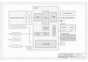
The layout will somewhat resemble the layout of the (virtual) DIY Calculator with an 20x1 character LC display and a 70 keys sensor key matrix. Additionally there are connectivity means for a host PC:
- Serial (RS-232) for uploading user programs and providing a console to the DIY Calculator CPU
- A JTAG programming connector; this connects to the PC's parallel port and enables the user to load new designs into the FPGA
- Additionally there will be sockets for external ROM/RAM chips and a large prototyping area for free use.
Download the detailed schematics from here: Schematics
Project status (19.Jul.2006): schematics completed, PCB layout work started
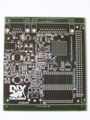
Project status (7.Aug.2006): We decided to separate the functionality into two PCBs: the FPGA with surrounding components and the sensor keypad. This gives even more flexibility for different I/O modules. Here are the updated schematics:
Project status (13.Aug.2006): Prototype PCB layout completed. Here are the "final" schematics:
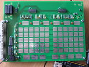
keypad mechanics:
and the layout:
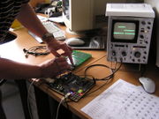
Test of sensor keypad is in progress.
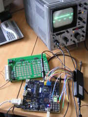
Project status (31.Aug.2006): Test of sensor keypad was successful. Here are the photos:
FPGA Project
The PCB will contain an FPGA chip in the 10K-gates size-class (Lattice LFEC10E-3F256C) with a 256 pin BGA footprint. The included JTAG connector makes this a development board for general use. With ispLEVER, the FPGA development software suite from Lattice Semiconductor, the FPGA design can be altered or a completely new design can be made. The entry level version of ispLEVER (ispLEVER-Starter) can be downloaded freely from Lattice. With Lattice's ispVM System the design can be transferred via JTAG to the DIY Calculator PCB.
The FPGA design of the DIY Calculator is based on the work of Steven Cooper, Carl Hoggins, Bjornar Prestegard, Svein Roar Kvaale, and Dr Albert Koelmans (instructor) of the University of Newcastle Upon Tyne, England.
Additionally to the CPU and ROM and RAM there will be special logic for the switch matrix, for LCD output, an a UART for RS-232 communication to the host PC.
Project status (19.Jul.2006): concept proved, integration of the existing VHDL design (was done with Altera/Quartus) into ispLEVER
Project status (7.Aug.2006): Simulation of the existing CPU design revealed big troubles. A new design of the CPU is being made.
Project status (31.Aug.2006): new CPU design is ready! (simulated and tested in a Lattice FPGA development board.)
Download the VHDL code from here: cpu.zip
Next steps are design/integration of:
- LCD controller
- UART
- Keypad controller
- stay tuned!
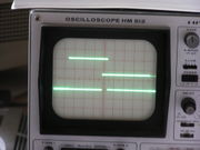
Notice that there are two access cycles to the LCD module with each character, one which actually writes the character and a second one which shifts the display left, mimicing the display behaviour of desktop calculators.
Also note that during LCD accesses the CPU is effectively halted by the nWAIT signal which is generated by the LCD controller. Between LCD accesses there is activity on the CPU data and address bus, which indictaes the loading of the next character, etc. View the "Hello World" program here: hello-tasm.lst
ROM Monitor Project
On of the primary goals of the DIY Calculator project is to teach how computers are working on machine language level ("How Computers Do Math"). So everyone is highly encouraged to translate various algorithms into assembly programs for the DIY Calculator. The current virtual DIY Calculator comes with a ready-to-use environment, which includes the calculator-like user interface, an assembler, a simulator, single-step debugger, and memory and register display. When translating the design to a physical one there has to be an environment, too. The most important functionality (and this is the only one being in scope of this project) is to run user programs to the DIY Calculator hardware. To be able to do that there must be means of:
- uploading the program to the hardware
- store it in some non-volatile storage
- actually run it
- obtain some status information (e.g. terminated correctly, does not fit into memory, etc.)
This is the objective of the ROM monitor. The ROM monitor is, as its name suggests, a program which resides within the ROM of the DIY Calculator. It is always present there and provides for the above mentioned supervising tasks. It uses the RS-232 port both for transferring the user program and as console port to which you can connect with a terminal emulation program (or a real "dumb" terminal if can get hold of one ..) to enter commands and display status information. The ROM monitor will be written in the DIY Calculator's assembly language and will additionally supply some basic functions (e.g. status/log output via RS-232) to user programs.
Project status (19.Jul.2006): basic conceptual design ready
Project status (7.Aug.2006): no changes
Project status (31.Aug.2006): no changes
Upload Utility Project
The user program upload process is handled by the ROM monitor on the DIY Calculator side. But there must be a means of sending a program to the DIY Calculator. While it is possible to send a file with the terminal emulation program a GUI program is preferable. Furthermore, by having a dedicated program for this task it is possible to generate a check sum or use a protocol of choice for ensuring correct transmission. The transmission status (success/failure) can be displayed. This program should be written in "C" using the GTK library of GUI widgets to be easily ported to different platforms.
Project status (19.Jul.2006): considered
Project status (7.Aug.2006): no changes
Project status (31.Aug.2006): no changes
